2025.12.18
お知らせ News
9/25(Thu.) ジョン・ローレンスJohn Lawrenceラピダス最新情報プリゼン
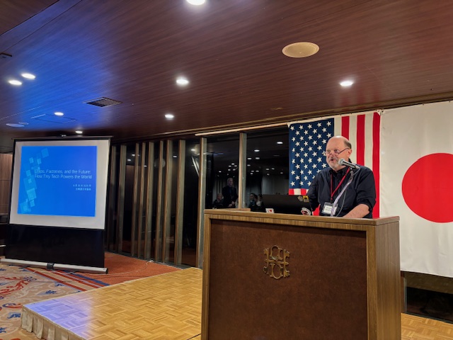
9月25日(木・札幌パークホテル)の例会には、半導体メーカーのラピダス社と国内外情報に詳しく、親日派で千歳在住のジョン・ローレンス氏をゲスト・スピーカーにお招きし講演会を開催しました。
Tiny tech, in the form of semiconductors, and how it powers the world was the theme of the Thursday, Sept. 25th Hokkaido Japan-U.S. Association Regular Meeting, as members heard from John Lawrence, a longtime American resident of Japan and semiconductor industry veteran who is one of the leading experts on the semiconductor industry.
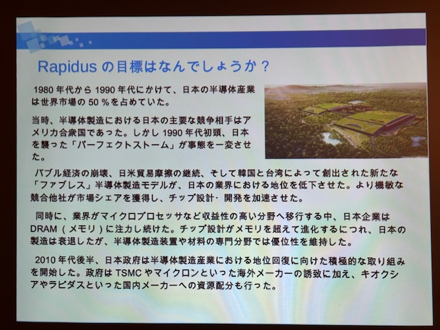
With the two-nanometer semiconductor chips scheduled to go into mass production at the Rapidus plant in Chitose in 2027, anticipation is high in Hokkaido, Japan, and around the world that the chips will reboot Japan’s domestic semiconductor manufacturing industry. But how many of us really have an understanding of how this critical technology works?
ローレンズさんは、世界に向けた同産業の未来や戦略について~半導体とあなた~小さな微粒子が、世界にどのようなインパクトを与えるのか?~」についてプリゼンテーションを行って頂きました。
In clear, jargon-free language, Mr. Lawrence took society members through a bilingual PowerPoint of the manufacturing process–from the moment a chip starts as a piece of ultrapure silicon in the form of an ingot, which is refined from sand, through a process that includes being sliced into thin wafers,putting layers of substrate, as well as conducting and insulating materials, to imprinting circuit patterns, to the final cleaning and inspection process to ensure there is no dust. Even a piece of dust 2 mn wide can damage the entire wafer, Mr. Lawrence said.
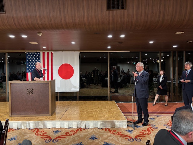
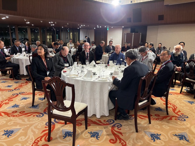
講演のハイライトは、ローレンズさんは、持参し参加者たちにプレゼントされた半導体チップをもとにプリゼンテーションを、わかりやすく展開されたことにつきます。今後、日本の大手企業のキャノンやソフトバンク、トヨタその他が出資する北海道発のラピダスの動きが世界でも注目されています。今回のローレンスさんをゲスト・スピーカー として招くにあたっては、その準備と英文編集等で、本協会の会員でザ・ジャパンタイムズの上特派員のエリック・ジョンストンさんにお世話になり感謝申し上げます。
The highlight of the presentation came when Mr. Lawrence asked participants to observe the tiny chip and small piece of paper taped inside the small, clear plastic box that had been on the tables in front of each participant. Imagine, he said, if that tiny little chip, not much larger than a large grain of sand, were blown up to an area that matches the land area of Japan, compressed into a square. That would be a chip 614.8 X 614.8 square kilometers–roughly the distance between the Sapporo Park Hotel and Minami Soma, Fukushima Prefecture going north to south.
On a chip the size of Japan, then, what would be the equivalent of two nanometers, which is what Rapidus is developing? Just 8.2 centimeters!
Mr. Lawrence also spoke on what was going on in other parts of Japan where semiconductor manufacturing plays an important role in the local economy. But he quoted a warning of a Kumamoto prefectural assemblyman who noted that while it was easy to set up a semiconductor factory if the government gives you money, staffing is impossible without a local investment in people.
But in a sense, this is a form of “good trouble” for local businesses, as it spurs older, stagnant economies to reinvent themselves. All of Hokkaido looks forward to the Rapidus project and hopes that it will be the centerpiece of a larger economic revitalization effort. Thanks to Mr. Lawrence’s excellent presentation, Hokkaido Japan-America Society members have a much better understanding of the semiconductor industry itself. We appreciate Eric Johnston(Senior National Correspondent of The Japan Times & our member) for his help and cooperation for inviting John Lawrence as a guest speaker and his editorial work .